How to Use Flags in Verilog Design
Verilog generate statement is a powerful construct for writing configurable, synthesizable RTL. It can be used to create multiple instantiations of modules and code, or conditionally instantiate blocks of code. However, many Verilog programmers often have questions about how to use Verilog generate effectively. In this article, I will review the usage of three forms of Verilog generate—generate loop, if-generate, and case-generate.
Types of Verilog Generate Constructs
There are two kinds of Verilog generate constructs. Generate loop constructs allow a block of code to be instantiated multiple times, controlled by a variable index. Conditional generate constructs select at most one block of code between multiple blocks. Conditional generate constructs include if-generate and case-generate forms.
Verilog generate constructs are evaluated at elaboration, which occurs after parsing the HDL (and preprocessor), but before simulation begins. Therefore all expressions within generate constructs must be constant expressions, deterministic at elaboration time. For example, generate constructs can be affected by values from parameters, but not by dynamic variables.
A Verilog generate block creates a new scope and a new level of hierarchy, almost like instantiating a module. This sometimes causes confusion when trying to write a hierarchical reference to signals or modules within a generate block, so it is something to keep in mind.
Use of the keywords generate and endgenerate (and begin/end) is actually optional. If they are used, then they define a generate region. Generate regions can only occur directly within a module, and they cannot nest. For readability, I like to use the generate and endgenerate keywords.
Verilog Generate Loop
The syntax for a generate loop is similar to that of a for loop statement. The loop index variable must first be declared in a genvar declaration before it can be used. The genvar is used as an integer to evaluate the generate loop during elaboration. The genvar declaration can be inside or outside the generate region, and the same loop index variable can be used in multiple generate loops, as long as the loops don't nest.
Within each instance of the "unrolled" generate loop, an implicit localparam is created with the same name and type as the loop index variable. Its value is the "index" of the particular instance of the "unrolled" loop. This localparam can be referenced from RTL to control the generated code, and even referenced by a hierarchical reference.
Generate block in a Verilog generate loop can be named or unnamed. If it is named, then an array of generate block instances is created. Some tools warn you about unnamed generate loops, so it is good practice to always name them.
The following example shows a gray to binary code converter written using a Verilog generate loop.
Example of parameterized gray to binary code converter module gray2bin #(parameter SIZE = 8) ( input [SIZE-1:0] gray, output [SIZE-1:0] bin ) Genvar gi; // generate and endgenerate is optional // generate (optional) for (gi=0; gi<SIZE; gi=gi+1) begin : genbit assign bin[gi] = ^gray[SIZE-1:gi]; // Thanks Dhruvkumar! end // endgenerate (optional) endmodule
Another example from the Verilog-2005 LRM illustrates how each iteration of the Verilog generate loop creates a new scope. Notice wire t1, t2, t3 are declared within the generate loop. Each loop iteration creates a new t1, t2, t3 that do not conflict, and they are used to wire one generated instance of the adder to the next. Also note the naming of the hierarchical reference to reference an instance within the generate loop.
module addergen1 #(parameter SIZE = 4) ( input logic [SIZE-1:0] a, b, input logic ci, output logic co, output logic [SIZE-1:0] sum ); wire [SIZE :0] c; genvar i; assign c[0] = ci; // Hierarchical gate instance names are: // xor gates: bitnum[0].g1 bitnum[1].g1 bitnum[2].g1 bitnum[3].g1 // bitnum[0].g2 bitnum[1].g2 bitnum[2].g2 bitnum[3].g2 // and gates: bitnum[0].g3 bitnum[1].g3 bitnum[2].g3 bitnum[3].g3 // bitnum[0].g4 bitnum[1].g4 bitnum[2].g4 bitnum[3].g4 // or gates: bitnum[0].g5 bitnum[1].g5 bitnum[2].g5 bitnum[3].g5 // Gate instances are connected with nets named: // bitnum[0].t1 bitnum[1].t1 bitnum[2].t1 bitnum[3].t1 // bitnum[0].t2 bitnum[1].t2 bitnum[2].t2 bitnum[3].t2 // bitnum[0].t3 bitnum[1].t3 bitnum[2].t3 bitnum[3].t3 for(i=0; i<SIZE; i=i+1) begin:bitnum wire t1, t2, t3; xor g1 ( t1, a[i], b[i]); xor g2 ( sum[i], t1, c[i]); and g3 ( t2, a[i], b[i]); and g4 ( t3, t1, c[i]); or g5 ( c[i+1], t2, t3); end assign co = c[SIZE]; endmodule
Generate loops can also nest. Only a single generate/endgenerate is needed (or none, since it's optional) to encompass the nested generate loops. Remember each generate loop creates a new scope. Therefore the hierarchical reference to the inner loop needs to include the label of the outer loop.
Conditional If-Generate
Conditional if-generate selects at most one generate block from a set of alternative generate blocks. Note I say at most, because it may also select none of the blocks. The condition must again be a constant expression during elaboration.
Conditional if-generate may be named or unnamed, and may or may not have begin/end. Either way, it can contain only one item. It also creates a separate scope and level of hierarchy, like a generate loop. Since conditional generate selects at most one block of code, it is legal to name the alternative blocks of code within the single if-generate with the same name. That helps to keep hierarchical reference to the code common regardless of which block of code is selected. Different generate constructs, however, must have different names.
Conditional Case-Generate
Similar to if-generate, case-generate can also be used to conditionally select one block of code from several blocks. Its usage is similar to the basic case statement, and all rules from if-generate also apply to case-generate.
Direct Nesting of Conditional Generate
There is a special case where nested conditional generate blocks that are not surrounded by begin/end can consolidate into a single scope/hierarchy. This avoids creating unnecessary scope/hierarchy within the module to complicate the hierarchical reference. This special case does not apply at all to loop generate.
The example below shows how this special rule can be used to construct complex if-else if conditional generate statements that belong to the same hierarchy.
module test; parameter p = 0, q = 0; wire a, b, c; //--------------------------------------------------------- // Code to either generate a u1.g1 instance or no instance. // The u1.g1 instance of one of the following gates: // (and, or, xor, xnor) is generated if // {p,q} == {1,0}, {1,2}, {2,0}, {2,1}, {2,2}, {2, default} //--------------------------------------------------------- if (p == 1) if (q == 0) begin : u1 // If p==1 and q==0, then instantiate and g1(a, b, c); // AND with hierarchical name test.u1.g1 end else if (q == 2) begin : u1 // If p==1 and q==2, then instantiate or g1(a, b, c); // OR with hierarchical name test.u1.g1 end // "else" added to end "if (q == 2)" statement else ; // If p==1 and q!=0 or 2, then no instantiation else if (p == 2) case (q) 0, 1, 2: begin : u1 // If p==2 and q==0,1, or 2, then instantiate xor g1(a, b, c); // XOR with hierarchical name test.u1.g1 end default: begin : u1 // If p==2 and q!=0,1, or 2, then instantiate xnor g1(a, b, c); // XNOR with hierarchical name test.u1.g1 end endcase endmodule This generate construct will select at most one of the generate blocks named u1. The hierarchical name of the gate instantiation in that block would be test.u1.g1. When nesting if-generate constructs, the else always belongs to the nearest if construct. Note the careful placement of begin/end within the code Any additional begin/end will violate the direct nesting requirements, and cause an additional hierarchy to be created.
Named vs Unnamed Generate Blocks
It is recommended to always name generate blocks to simplify hierarchical reference. Moreover, various tools often complain about anonymous generate blocks. However, if a generate block is unnamed, the LRM does describe a fixed rule for how tools shall name an anonymous generate block based on the text of the RTL code.
First, each generate construct in a scope is assigned a number, starting from 1 for the generate construct that appears first in the RTL code within that scope, and increases by 1 for each subsequent generate construct in that scope. The number is assigned to both named and unnamed generate constructs. All unnamed generate blocks will then be given the name genblk[n] where [n] is the number assigned to its enclosing generate construct.
It is apparent from the rule that RTL code changes will cause the unnamed generate construct name to change. That in turn makes it difficult to maintain hierarchical references in RTL and scripts. Therefore, it is recommended to always name generate blocks.
Conclusion
Verilog generate constructs are powerful ways to create configurable RTL that can have different behaviours depending on parameterization. Generate loop allows code to be instantiated multiple times, controlled by an index. Conditional generate, if-generate and case-generate, can conditionally instantiate code. The most important recommendation regarding generate constructs is to always name them, which helps simplify hierarchical references and code maintenance.
References
- 1364-2005 – IEEE Standard for Verilog Hardware Description Language
- Author
- Recent Posts

Jason has 10 years' experience in the semiconductor industry, designing and verifying Solid State Drive controller SoC. His areas of workinclude microarchitecture and RTL design, dynamic and formal verification using UVM and Cadence JasperGold, and full-chip low power verification with UPF. Thoughts and opinions expressed in articles are personal and do not reflect that of Intel Corporation in any way.
In my last article on plain old Verilog Arrays, I discussed their very limited feature set. In comparison, SystemVerilog arrays have greatly expanded capabilities both for writing synthesizable RTL, and for writing non-synthesizable test benches. In this article, we'll take a look at the synthesizable features of SystemVerilog Arrays we can use when writing design RTL.
Packed vs Unpacked SystemVerilog Arrays
Verilog had only one type of array. SystemVerilog arrays can be either packed or unpacked. Packed array refers to dimensions declared after the type and before the data identifier name. Unpacked array refers to the dimensions declared after the data identifier name.
bit [7:0] c1; // packed array of scalar bit real u [7:0]; // unpacked array of real int Array[0:7][0:31]; // unpacked array declaration using ranges int Array[8][32]; // unpacked array declaration using sizes
Packed Arrays
A one-dimensional packed array is also called a vector. Packed array divides a vector into subfields, which can be accessed as array elements. A packed array is guaranteed to be represented as a contiguous set of bits in simulation and synthesis.
Packed arrays can be made of only the single bit data types (bit, logic, reg), enumerated types, and other packed arrays and packed structures. This also means you cannot have packed arrays of integer types with predefined widths (e.g. a packed array of byte).
Unpacked arrays
Unpacked arrays can be made of any data type. Each fixed-size dimension is represented by an address range, such as [0:1023], or a single positive number to specify the size of a fixed-size unpacked array, such as [1024]. The notation [size] is equivalent to [0:size-1].
Indexing and Slicing SystemVerilog Arrays
Verilog arrays could only be accessed one element at a time. In SystemVerilog arrays, you can also select one or more contiguous elements of an array. This is called a slice. An array slice can only apply to one dimension; other dimensions must have single index values in an expression.
Multidimensional Arrays
Multidimensional arrays can be declared with both packed and unpacked dimensions. Creating a multidimensional packed array is analogous to slicing up a continuous vector into multiple dimensions.
When an array has multiple dimensions that can be logically grouped, it is a good idea to use typedef to define the multidimensional array in stages to enhance readability.
bit [3:0] [7:0] joe [0:9] // 10 elements of 4 8-bit bytes // (each element packed into 32 bits) typedef bit [4:0] bsix; // multiple packed dimensions with typedef bsix [9:0] v5; // equivalent to bit[4:0][9:0] v5 typedef bsix mem_type [0:3]; // array of four unpacked 'bsix' elements mem_type ba [0:7]; // array of eight unpacked 'mem_type' elements // equivalent to bit[4:0] ba [0:3][0:7] - thanks Dennis!
SystemVerilog Array Operations
SystemVerilog arrays support many more operations than their traditional Verilog counterparts.
+: and -: Notation
When accessing a range of indices (a slice) of a SystemVerilog array, you can specify a variable slice by using the [start+:increment width] and [start-:decrement width] notations. They are simpler than needing to calculate the exact start and end indices when selecting a variable slice. The increment/decrement width must be a constant.
bit signed [31:0] busA [7:0]; // unpacked array of 8 32-bit vectors int busB [1:0]; // unpacked array of 2 integers busB = busA[7:6]; // select a 2-vector slice from busA busB = busA[6+:2]; // equivalent to busA[7:6]; typo fixed, thanks Tomer!
Assignments, Copying, and other Operations
SystemVerilog arrays support many more operations than Verilog arrays. The following operations can be performed on both packed and unpacked arrays.
A = B; // reading and writing the array A[i:j] = B[i:j]; // reading and writing a slice of the array A[x+:c] = B[y+:d]; // reading and writing a variable slice of the array A[i] = B[i]; // accessing an element of the array A == B; // equality operations on the array A[i:j] != B[i:j]; // equality operations on slice of the array
Packed Array Assignment
A SystemVerilog packed array can be assigned at once like a multi-bit vector, or also as an individual element or slice, and more.
logic [1:0][1:0][7:0] packed_3d_array; always_ff @(posedge clk, negedge rst_n) if (!rst_n) begin packed_3d_array <= '0; // assign 0 to all elements of array end else begin packed_3d_array[0][0][0] <= 1'b0; // assign one bit packed_3d_array[0][0] <= 8'h0a; // assign one element packed_3d_array[0][0][3:0] <= 4'ha; // assign part select packed_3d_array[0] <= 16'habcd; // assign slice packed_3d_array <= 32'h01234567; // assign entire array as vector end
Unpacked Array Assignment
All or multiple elements of a SystemVerilog unpacked array can be assigned at once to a list of values. The list can contain values for individual array elements, or a default value for the entire array.
logic [7:0] a, b, c; logic [7:0] d_array[0:3]; logic [7:0] e_array[3:0]; // note index of unpacked dimension is reversed // personally, I prefer this form logic [7:0] mult_array_a[3:0][3:0]; logic [7:0] mult_array_b[3:0][3:0]; always_ff @(posedge clk, negedge rst_n) if (!rst_n) begin d_array <= '{default:0}; // assign 0 to all elements of array end else begin d_array <= '{8'h00, c, b, a}; // d_array[0]=8'h00, d_array[1]=c, d_array[2]=b, d_array[3]=a e_array <= '{8'h00, c, b, a}; // e_array[3]=8'h00, e_array[2]=c, e_array[1]=b, d_array[0]=a mult_array_a <= '{'{8'h00, 8'h01, 8'h02, 8'h03}, '{8'h04, 8'h05, 8'h06, 8'h07}, '{8'h08, 8'h09, 8'h0a, 8'h0b}, '{8'h0c, 8'h0d, 8'h0e, 8'h0f}}; // assign to full array mult_array_b[3] <= '{8'h00, 8'h01, 8'h02, 8'h03}; // assign to slice of array end Conclusion
This article described the two new types of SystemVerilog arrays---packed and unpacked---as well as the many new features that can be used to manipulate SystemVerilog arrays. The features described in this article are all synthesizable, so you can safely use them in SystemVerilog based RTL designs to simplify coding. In the next part of the SystemVerilog arrays article, I will discuss more usages of SystemVerilog arrays that can make your SystemVerilog design code even more efficient. Stay tuned!
Resources
- Synthesizing SystemVerilog: Busting the Myth that SystemVerilog is only for Verification
- 1888-2012 IEEE Standard for SystemVerilog
- SystemVerilog for Design Second Edition:
A Guide to Using SystemVerilog for Hardware Design and Modeling
Sample Source Code
The accompany source code for this article is a toy example module and testbench that illustrates SystemVerilog array capabilities, including using an array as a port, assigning multi-dimensional arrays, and assigning slices of arrays. Download and run it to see how it works!
Download Article Companion Source Code
Get the FREE, EXECUTABLE test bench and source code for this article, notification of new articles, and more!
.
- Author
- Recent Posts
Jason has 10 years' experience in the semiconductor industry, designing and verifying Solid State Drive controller SoC. His areas of workinclude microarchitecture and RTL design, dynamic and formal verification using UVM and Cadence JasperGold, and full-chip low power verification with UPF. Thoughts and opinions expressed in articles are personal and do not reflect that of Intel Corporation in any way.
Arrays are an integral part of many modern programming languages. Verilog arrays are quite simple; the Verilog-2005 standard has only 2 pages describing arrays, a stark contrast from SystemVerilog-2012 which has 20+ pages on arrays. Having a good understanding of what array features are available in plain Verilog will help understand the motivation and improvements introduced in SystemVerilog. In this article I will restrict the discussion to plain Verilog arrays, and discuss SystemVerilog arrays in an upcoming post.
Verilog Arrays
Verilog arrays can be used to group elements into multidimensional objects to be manipulated more easily. Since Verilog does not have user-defined types, we are restricted to arrays of built-in Verilog types like nets, regs, and other Verilog variable types.
Each array dimension is declared by having the min and max indices in square brackets. Array indices can be written in either direction:
array_name[least_significant_index:most_significant_index], e.g. array1[0:7] array_name[most_significant_index:least_significant_index], e.g. array2[7:0] Personally I prefer the array2 form for consistency, since I also write vector indices (square brackets before the array name) in [most_significant:least_significant] form. However, this is only a preference not a requirement.
A multi-dimensional array can be declared by having multiple dimensions after the array declaration. Any square brackets before the array identifier is part of the data type that is being replicated in the array.
The Verilog-2005 specification also calls a one-dimensional array with elements of type reg a memory. It is useful for modeling memory elements like read-only memory (ROM), and random access memory (RAM).
Verilog arrays are synthesizable, so you can use them in synthesizable RTL code.
reg [31:0] x[127:0]; // 128-element array of 32-bit wide reg wire[15:0] y[ 7:0], z[7:0]; // 2 arrays of 16-bit wide wires indexed from 7 to 0 reg [ 7:0] mema [255:0]; // 256-entry memory mema of 8-bit registers reg arrayb [ 7:0][255:0]; // two-dimensional array of one bit registers Assigning and Copying Verilog Arrays
Verilog arrays can only be referenced one element at a time. Therefore, an array has to be copied a single element at a time. Array initialization has to happen a single element at a time. It is possible, however, to loop through array elements with a generate or similar loop construct. Elements of a memory must also be referenced one element at a time.
initial begin mema = 0; // Illegal syntax - Attempt to write to entire array arrayb[1] = 0; // Illegal syntax - Attempt to write to elements [1][255]...[1][0] arrayb[1][31:12] = 0; // Illegal syntax - Attempt to write to multiple elements mema[1] = 0; // Assigns 0 to the second element of mema arrayb[1][0] = 0; // Assigns 0 to the bit referenced by indices [1][0] end // Generate loop with arrays of wires generate genvar gi; for (gi=0; gi<8; gi=gi+1) begin : gen_array_transform my_example_16_bit_transform_module u_mod ( .in (y[gi]), .out (z[gi]) ); end endgenerate // For loop with arrays integer index; always @(posedge clk, negedge rst_n) begin if (!rst_n) begin // reset arrayb for (index=0; index<256; index=index+1) begin mema[index] <= 8'h00; end end else begin // out of reset functional code end end
Conclusion
Verilog arrays are plain, simple, but quite limited. They really do not have many features beyond the basics of grouping signals together into a multidimensional structure. SystemVerilog arrays, on the other hand, are much more flexible and have a wide range of new features and uses. In the next article—SystemVerilog arrays, Synthesizable and Flexible—I will discuss the new features that have been added to SystemVerilog arrays and how to use them.
References
- 1364-2005 – IEEE Standard for Verilog Hardware Description Language
Sample Source Code
The accompany source code for this article is a toy example module and testbench that illustrates SystemVerilog array capabilities, including using an array as a port, assigning multi-dimensional arrays, and assigning slices of arrays. Download and run it to see how it works!
Download Article Companion Source Code
Get the FREE, EXECUTABLE test bench and source code for this article, notification of new articles, and more!
.
- Author
- Recent Posts
Jason has 10 years' experience in the semiconductor industry, designing and verifying Solid State Drive controller SoC. His areas of workinclude microarchitecture and RTL design, dynamic and formal verification using UVM and Cadence JasperGold, and full-chip low power verification with UPF. Thoughts and opinions expressed in articles are personal and do not reflect that of Intel Corporation in any way.
The difference between Verilog reg and Verilog wire frequently confuses many programmers just starting with the language (certainly confused me!). As a beginner, I was told to follow these guidelines, which seemed to generally work:
- Use Verilog reg for left hand side (LHS) of signals assigned inside in always blocks
- Use Verilog wire for LHS of signals assigned outside always blocks
Then when I adopted SystemVerilog for writing RTL designs, I was told everything can now be "type logic". That again generally worked, but every now and then I would run into a cryptic error message about variables, nets, and assignment.
So I decided to find out exactly how these data types worked to write this article. I dug into the language reference manual, searched for the now-defunct Verilog-2005 standard document, and got into a bit of history lesson. Read on for my discovery of the differences between Verilog reg, Verilog wire, and SystemVerilog logic.
Verilog data types, Verilog reg, Verilog wire
Verilog data types are divided into two main groups: nets and variables. The distinction comes from how they are intended to represent different hardware structures.
A net data type represents a physical connection between structural entities (think a plain wire), such as between gates or between modules. It does not store any value. Its value is derived from what is being driven from its driver(s). Verilog wire is probably the most common net data type, although there are many other net data types such as tri, wand, supply0.
A variable data type generally represents a piece of storage. It holds a value assigned to it until the next assignment. Verilog reg is probably the most common variable data type. Verilog reg is generally used to model hardware registers (although it can also represent combinatorial logic, like inside an always@(*) block). Other variable data types include integer, time, real, realtime.
Almost all Verilog data types are 4-state, which means they can take on 4 values:
- 0 represents a logic zero, or a false condition
- 1 represents a logic one, or a true condition
- X represents an unknown logic value
- Z represents a high-impedance state
Verilog rule of thumb 1: use Verilog reg when you want to represent a piece of storage, and use Verilog wire when you want to represent a physical connection.
Assigning values to Verilog reg, Verilog wire
Verilog net data types can only be assigned values by continuous assignments. This means using constructs like continuous assignment statement (assign statement), or drive it from an output port. A continuous assignment drives a net similar to how a gate drives a net. The expression on the right hand side can be thought of as a combinatorial circuit that drives the net continuously.
Verilog variable data types can only be assigned values using procedural assignments. This means inside an always block, an initial block, a task, a function. The assignment occurs on some kind of trigger (like the posedge of a clock), after which the variable retains its value until the next assignment (at the next trigger). This makes variables ideal for modeling storage elements like flip-flops.
Verilog rule of thmb 2: drive a Verilog wire with assign statement or port output, and drive a Verilog reg from an always block. If you want to drive a physical connection with combinatorial logic inside an always@(*) block, then you have to declare the physical connection as Verilog reg.
SystemVerilog logic, data types, and data objects
SystemVerilog introduces a new 2-state data type—where only logic 0 and logic 1 are allowed, not X or Z—for testbench modeling. To distinguish the old Verilog 4-state behaviour, a new SystemVerilog logic data type is added to describe a generic 4-state data type.
What used to be data types in Verilog, like wire, reg, wand, are now called data objects in SystemVerilog. Wire, reg, wand (and almost all previous Verilog data types) are 4-state data objects. Bit, byte, shortint, int, longint are the new SystemVerilog 2-state data objects.
There are still the two main groups of data objects: nets and variables. All the Verilog data types (now data objects) that we are familiar with, since they are 4-state, should now properly also contain the SystemVerilog logic keyword.
wire my_wire; // implicitly means "wire logic my_wire" wire logic my_wire; // you can also declare it this way wire [7:0] my_wire_bus; // implicitly means "wire logic[15:0] my_wire_bus" wire logic [7:0] my_wire_logic_bus; // you can also declare it this way reg [15:0] my_reg_bus; // implicitly means "reg logic[15:0] my_reg_bus" //reg logic [15:0] my_reg_bus; // but if you declare it fully, VCS 2014.10 doesn't like it
There is a new way to declare variables, beginning with the keyword var. If the data type (2-state or 4-state) is not specified, then it is implicitly declared as logic. Below are some variable declaration examples. Although some don't seem to be fully supported by tools.
// From the SV-2012 LRM Section 6.8 var byte my_byte; // byte is 2-state, so this is a variable // var v; // implicitly means "var logic v;", but VCS 2014.10 doesn't like this var logic v; // this is okay // var [15:0] vw; // implicitly means "var logic [15:0] vw;", but VCS 2014.10 doesn't like this var logic [15:0] vw; // this is okay var enum bit {clear, error} status; // variable of enumerated type var reg r; // variable reg Don't worry too much about the var keyword. It was added for language preciseness (it's what happens as a language evolves and language gurus strive to maintain backward-compatibility), and you'll likely not see it in an RTL design.
I'm confused… Just tell me how I should use SystemVerilog logic!
After all that technical specification gobbledygook, I have good news if you're using SystemVerilog for RTL design. For everyday usage in RTL design, you can pretty much forget all of that!
The SystemVerilog logic keyword standalone will declare a variable, but the rules have been rewritten such that you can pretty much use a variable everywhere in RTL design. Hence, you see in my example code from other articles, I use SystemVerilog logic to declare variables and ports.
module my_systemverilog_module ( input logic clk, input logic rst_n, input logic data_in_valid, input logic [7:0] data_in_bus, output logic data_out_valid, // driven by always_ff, it is a variable output logic [7:0] data_out_bus, // driven by always_comb, it is a variable output logic data_out_err // also a variable, driven by continuous assignment (allowed in SV) ); assign data_out_err = 1'b1; // continuous assignment to a variable (allowed in SV) // always_comb data_out_err = 1'b0; // multiple drivers to variable not allowed, get compile time error always_comb data_out_bus = <data_out_bus logic expression>; always_ff @(posedge clk, negedge rst_n) if (!rst_n) data_out_valid <= 1'b0; else data_out_valid <= <data_out_valid logic expression>; endmodule
When you use SystemVerilog logic standalone this way, there is another advantage of improved checking for unintended multiple drivers. Multiple assignments, or mixing continuous and procedural (always block) assignments, to a SystemVerilog variable is an error, which means you will most likely see a compile time error. Mixing and multiple assignments is allowed for a net. So if you really want a multiply-driven net you will need to declare it a wire.
In Verilog it was legal to have an assignment to a module output port (declared as Verilog wire or Verilog reg) from outside the module, or to have an assignment inside the module to a net declared as an input port. Both of these are frequently unintended wiring mistakes, causing contention. With SystemVerilog, an output port declared as SystemVerilog logic variable prohibits multiple drivers, and an assignment to an input port declared as SystemVerilog logic variable is also illegal. So if you make this kind of wiring mistake, you will likely again get a compile time error.
SystemVerilog rule of thumb 1: if using SystemVerilog for RTL design, use SystemVerilog logic to declare:
- All point-to-point nets. If you specifically need a multi-driver net, then use one of the traditional net types like wire
- All variables (logic driven by always blocks)
- All input ports
- All output ports
If you follow this rule, you can pretty much forget about the differences between Verilog reg and Verilog wire! (well, most of the time)
Conclusion
When I first wondered why it was possible to always write RTL using SystemVerilog logic keyword, I never expected it to become a major undertaking that involved reading and interpreting two different specifications, understanding complex language rules, and figuring out their nuances. At least I can say that the recommendations are easy to remember.
I hope this article gives you a good summary of Verilog reg, Verilog wire, SystemVerilog logic, their history, and a useful set of recommendations for RTL coding. I do not claim to be a Verilog or SystemVerilog language expert, so please do correct me if you felt I misinterpreted anything in the specifications.
References
- Synthesizing SystemVerilog : Busting the Myth that SystemVerilog is only for Verification
- 1800-2012 – IEEE Standard for SystemVerilog–Unified Hardware Design, Specification, and Verification Language
- 1364-2005 – IEEE Standard for Verilog Hardware Description Language
- A lively discussion in Google Groups on SystemVerilog var keyword
Sample Source Code
The accompanying source code for this article is a SystemVerilog design and testbench toy example that demonstrates the difference between using Verilog reg, Verilog wire, and SystemVerilog logic to code design modules. Download the code to see how it works!
Download Article Companion Source Code
Get the FREE, EXECUTABLE test bench and source code for this article, notification of new articles, and more!
.
- Author
- Recent Posts
Jason has 10 years' experience in the semiconductor industry, designing and verifying Solid State Drive controller SoC. His areas of workinclude microarchitecture and RTL design, dynamic and formal verification using UVM and Cadence JasperGold, and full-chip low power verification with UPF. Thoughts and opinions expressed in articles are personal and do not reflect that of Intel Corporation in any way.
SystemVerilog struct (ure) and union are very similar to their C programming counterparts, so you may already have a good idea of how they work. But have you tried using them in your RTL design? When used effectively, they can simplify your code and save a lot of typing. Recently, I tried incorporating SystemVerilog struct and union in new ways that I had not done before with surprisingly (or not surprisingly?) good effect. In this post I would like to share with you some tips on how you can also use them in your RTL design.
What is a SystemVerilog Struct (ure)?
A SystemVerilog struct is a way to group several data types. The entire group can be referenced as a whole, or the individual data type can be referenced by name. It is handy in RTL coding when you have a collection of signals you need to pass around the design together, but want to retain the readability and accessibility of each separate signal.
When used in RTL code, a packed SystemVerilog struct is the most useful. A packed struct is treated as a single vector, and each data type in the structure is represented as a bit field. The entire structure is then packed together in memory without gaps. Only packed data types and integer data types are allowed in a packed struct. Because it is defined as a vector, the entire structure can also be used as a whole with arithmetic and logical operators.
An unpacked SystemVerilog struct, on the other hand, does not define a packing of the data types. It is tool-dependent how the structure is packed in memory. Unpacked struct probably will not synthesize by your synthesis tool, so I would avoid it in RTL code. It is, however, the default mode of a structure if the packed keyword is not used when defining the structure.
SystemVerilog struct is often defined with the typedef keyword to give the structure type a name so it can be more easily reused across multiple files. Here is an example:
typedef enum logic[15:0] { ADD = 16'h0000, SUB = 16'h0001 } my_opcode_t; typedef enum logic[15:0] { REG = 16'h0000, MEM = 16'h0001 } my_dest_t; typedef struct packed { my_opcode_t opcode; // 16-bit opcode, enumerated type my_dest_t dest; // 16-bit destination, enumerated type logic [15:0] opA; logic [15:0] opB; } my_opcode_struct_t; my_opcode_struct_t cmd1; initial begin // Access fields by name cmd1.opcode <= ADD; cmd1.dest <= REG; cmd1.opA <= 16'h0001; cmd1.opB <= 16'h0002; // Access fields by bit position cmd1[63:48] <= 16'h0000 cmd1[47:32] <= 16'h0000; cmd1[31:16] <= 16'h0003; cmd1[15: 0] <= 16'h0004; // Assign fields at once cmd1 <= '{SUB, REG, 16'h0005, 16'h0006}; end What is a SystemVerilog Union?
A SystemVerilog union allows a single piece of storage to be represented different ways using different named member types. Because there is only a single storage, only one of the data types can be used at a time. Unions can also be packed and unpacked similarly to structures. Only packed data types and integer data types can be used in packed union. All members of a packed (and untagged, which I'll get to later) union must be the same size. Like packed structures, packed union can be used as a whole with arithmetic and logical operators, and bit fields can be extracted like from a packed array.
A tagged union is a type-checked union. That means you can no longer write to the union using one member type, and read it back using another. Tagged union enforces type checking by inserting additional bits into the union to store how the union was initially accessed. Due to the added bits, and inability to freely refer to the same storage using different union members, I think this makes it less useful in RTL coding.
Take a look at the following example, where I expand the earlier SystemVerilog struct into a union to provide a different way to access that same piece of data.
typedef union packed { my_opcode_struct_t opcode_s; "fields view" to the struct logic[1:0][31:0] dword; // "dword view" to the struct } my_opcode_union_t; my_opcode_union_t cmd2; initial begin // Access opcode_s struct fields within the union cmd2.opcode_s.opcode = ADD; cmd2.opcode_s.dest = REG; cmd2.opcode_s.opA = 16'h0001; cmd2.opcode_s.opB = 16'h0002; // Access dwords struct fields within the union cmd2.dword[1] = 32'h0001_0001; // opcode=SUB, dest=MEM cmd2.dword[0] = 32'h0007_0008; // opA=7, opB=8 end Ways to Use SystemVerilog Struct in a Design
There are many ways to incorporate SystemVerilog struct into your RTL code. Here are some common usages.
Encapsulate Fields of a Complex Type
One of the simplest uses of a structure is to encapsulate signals that are commonly used together into a single unit that can be passed around the design more easily, like the opcode structure example above. It both simplifies the RTL code and makes it more readable. Simulators like Synopsys VCS will display the fields of a structure separately on a waveform, making the structure easily readable.
If you need to use the same structure in multiple modules, a tip is to put the definition of the structure (defined using typedef) into a SystemVerilog package, then import the package into each RTL module that requires the definition. This way you will only need to define the structure once.
SystemVerilog Struct as a Module Port
A module port can have a SystemVerilog struct type, which makes it easy to pass the same bundle of signals into and out of multiple modules, and keep the same encapsulation throughout a design. For example a wide command bus between two modules with multiple fields can be grouped into a structure to simplify the RTL code, and to avoid having to manually decode the bits of the command bus when viewing it on a waveform (a major frustration!).
Using SystemVerilog Struct with Parameterized Data Type
A structure can be used effectively with modules that support parameterized data type. For example if a FIFO module supports parameterized data type, the entire structure can be passed into the FIFO with no further modification to the FIFO code.
module simple_fifo ( parameter type DTYPE = logic[7:0], parameter DEPTH = 4 ) ( input logic clk, input logic rst_n, input logic push, input logic pop, input DTYPE data_in, output logic[$clog2(DEPTH+1)-1:0] count, output DTYPE data_out ); // rest of FIFO design endmodule module testbench; parameter MY_DEPTH = 4; logic clk, rst_n, push, pop, full, empty; logic [$clog2(MY_DEPTH+1)-1:0] count; my_opcode_struct_t data_in, data_out; simple_fifo #( .DTYPE (my_opcode_struct_t), .DEPTH (MY_DEPTH) ) my_simple_fifo (.*); endmodule
Ways to Use SystemVerilog Union in a Design
Until very recently, I had not found a useful way to use a SystemVerilog union in RTL code. But I finally did in my last project! The best way to think about a SystemVerilog union is that it can give you alternative views of a common data structure. The packed union opcode example above has a "fields view" and a "dword view", which can be referred to in different parts of a design depending on which is more convenient. For example, if the opcode needs to be buffered in a 64-bit buffer comprised of two 32-bit wide memories, then you can assign one dword from the "dword view" as the input to each memory, like this:
my_opcode_union_t my_opcode_in, my_opcode_out; // Toy code to assign some values into the union always_comb begin my_opcode_in.opcode_s.opcode = ADD; my_opcode_in.opcode_s.dest = REG; my_opcode_in.opcode_s.opA = 16'h0001; my_opcode_in.opcode_s.opB = 16'h0002; end // Use the "dword view" of the union in a generate loop generate genvar gi; for (gi=0; gi<2; gi=gi+1) begin : gen_mem // instantiate a 32-bit memory mem_32 u_mem ( .D (my_opcode_in.dword[gi]), .Q (my_opcode_out.dword[gi]), .* ); end // gen_mem endgenerate
In my last project, I used a union this way to store a wide SystemVerilog struct into multiple 39-bit memories in parallel (32-bit data plus 7-bit SECDED encoding). The memories were divided this way such that each 32-bit dword can be individually protected by SECDED encoding so it is individually accessible by a CPU. I used a "dword view" of the union in a generate loop to feed the data into the SECDED encoders and memories. It eliminated alot of copying and pasting, and made the code much more concise!
Conclusion
SystemVerilog struct and union are handy constructs that can encapsulate data types and simplify your RTL code. They are most effective when the structure or union types can be used throughout a design, including as module ports, and with modules that support parameterized data types.
Do you have another novel way of using SystemVerilog struct and union? Leave a comment below!
References
- IEEE Standard for SystemVerilog 1800-2012
Download Article Companion Source Code
Get the FREE, EXECUTABLE test bench and source code for this article, notification of new articles, and more!
.
- Author
- Recent Posts
Jason has 10 years' experience in the semiconductor industry, designing and verifying Solid State Drive controller SoC. His areas of workinclude microarchitecture and RTL design, dynamic and formal verification using UVM and Cadence JasperGold, and full-chip low power verification with UPF. Thoughts and opinions expressed in articles are personal and do not reflect that of Intel Corporation in any way.
In Clock Domain Crossing (CDC) Design – Part 2, I discussed potential problems with passing multiple signals across a clock domain, and one effective and safe way to do so. That circuit, however, does hot handle the case when the destination side logic cannot accept data and needs to back-pressure the source side. The two feedback schemes in this article add this final piece.
The concepts in this article are again taken from Cliff Cummings' very comprehensive paper Clock Domain Crossing (CDC) Design & Verification Techniques Using SystemVerilog. I highly recommend taking an hour or two to read through it.
Multi-cycle path (MCP) formulation with feedback
How can the source domain logic know when it is safe to send the next piece of data to the synchronizer? It can wait a fixed number of cycles, which can be determined from the synchronizer circuit. But a better way is to have logic in the synchronizer to indicate this to the source domain. The following figure illustrates how this can be done. Compared to the MCP without feedback circuit, it adds a 1-bit finite state machine (FSM) to indicate to the source domain whether the synchronizer is ready to accept a new piece of data.

The 1-bit FSM has 2 states, 2 inputs, and 1 output (besides clock and reset).
- States: Idle, Busy
- Inputs: src_send, src_ack
- Output: src_rdy
The logic is simple. src_send causes the FSM to transition to Busy, src_ack causes the FSM to transition back to Idle. src_rdy output is 1 when Idle, and 0 when Busy. The user logic outside the synchronizer needs to monitor these signals to determine when it is safe to send a new piece of data.
Multi-cycle path (MCP) formulation with feedback acknowledge
What if the destination domain further needs to back-pressure data from the source domain? To do so, the destination domain will need control over when to send feedback acknowledgement to the source domain. This can be accomplished by adding a similar 1-bit FSM in the destination side of the synchronizer. This addition allows the destination clock domain to throttle the source domain to not send any data until the destination domain logic is ready. The following figure illustrates this design.

And there you have it. A complete multi-bit synchronizer solution with handshaking. Note that this particular design is slightly different from the design described in Cliff Cummings' paper. I have changed the destination side to output data on dest_data_out as soon as available, rather than waiting for an external signal to load the data like the bload signal in Cliff Cummings' circuit. It doesn't seem efficient to me to incur another cycle to make the data available.
I apologize that the diagram is a bit messy (if anyone knows of a better circuit drawing tool, please let me know). The source code will be provided below so you can study that in detail.
1-Deep Asynchronous FIFO
Obviously the dual-clock asynchronous FIFO can also be used to pass multiple bits across a clock domain crossing (CDC). What is interesting, however, is a 1-deep asynchronous FIFO (which actually has space for 2 entries, but will only ever fill 1 at a time) provides the same feedback acknowledge capability as the MCP formulation circuit above, but with 1 cycle lower latency on both the send and feedback paths.
In this configuration, pointers to the FIFO become single bit only, and toggle between 0 and 1. Read and write pointer comparison is redefined to produce a single bit value that indicates either ready to receive data (FIFO is empty, pointers equal) or not ready to receive data (FIFO is not empty, pointers not equal). Notice that when the logic indicates not ready, the write pointer has already incremented and is pointing to the next entry of the 2-entry storage to store data. Also, the FIFO read/write pointer circuitry essentially replaces the 1-bit state machine in the MCP formulation feedback scheme, therefore requiring 1 less step and 1 less cycle.
Conclusion
Over this 3-part series, we have looked at potential problems and proven design techniques to handle clock domain crossing (CDC) logic for single-bit signals (Part 1), and multi-bit signals (Part 2, and Part 3). Cliff Cummings gives a good summary from his paper:
Recommended 1-bit CDC techniques
- Register the signal in the source domain to remove combinational settling (glitches)
- Synchronize the signal into the destination domain
Recommended multi-bit CDC techniques
- Consolidate multiple signals into a 1-bit representation, then synchronize the 1-bit signal
- Use multi-cycle path (MCP) formulation to pass multi-bit data buses
- Use asynchronous FIFOs to pass multi-bit data or control buses
- Use gray code counters
Writing about this topic has been a much bigger (but also more rewarding) undertaking than I imagined. I must confess I'm still relatively new to asynchronous designs. So if you have any experience or design techniques to share, please leave a comment below! How about investigating clock domain crossing verification next?
References
- Clock Domain Crossing (CDC) Design & Verification Techniques Using SystemVerilog
- Simulation and Synthesis Techniques for Asynchronous FIFO Design
Sample Source Code
The accompanying source code for this article is the MCP feedback acknowledge synchronizer design and testbench, which generates the following waveform when run. Download and run the code to see how it works!

Download Article Companion Source Code
Get the FREE, EXECUTABLE test bench and source code for this article, notification of new articles, and more!
.
- Author
- Recent Posts
Jason has 10 years' experience in the semiconductor industry, designing and verifying Solid State Drive controller SoC. His areas of workinclude microarchitecture and RTL design, dynamic and formal verification using UVM and Cadence JasperGold, and full-chip low power verification with UPF. Thoughts and opinions expressed in articles are personal and do not reflect that of Intel Corporation in any way.
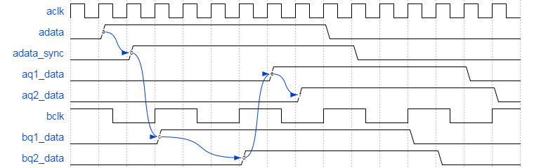
In Clock Domain Crossing (CDC) Techniques – Part 1, I briefly discussed metastability and two methods to safely synchronize a single bit. While those techniques are commonly used, in many applications we need to synchronize multiple control or data bits, like an encoded state or a data bus. Synchronizing multiple bits brings a host of other potential problems that need to be carefully examined, and solutions that build upon the basic blocks we discussed in part 1.
The concepts in this article are again mostly taken from Cliff Cumming's very comprehensive paper Clock Domain Crossing (CDC) Design & Verification Techniques Using SystemVerilog. I highly recommend taking an hour or two to read through it.
Problems With Passing Multiple Control Signals Across Clock Domain Crossing (CDC)
The fundamental problem with passing multiple bits is if they are synchronized individually, they cannot be guaranteed to arrive in the destination clock domain on the same clock edge. When the individual bits are launched from the source clock domain, they may be skewed relative to each other due to trace length, process variation, etc. Since in an asynchronous clock domain crossing (CDC) the destination clock can have every possible alignment relative to the source clock (and relative to the skewed data bits), the destination clock can (and will) sample at a time when not all the bits are at their stable final values. Therefore synchronizing individual bits of a multi-bit signal is not sufficient! Let's look at several potential problems.
Two simultaneously required signals
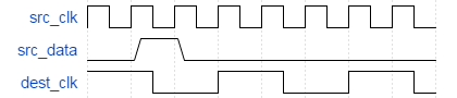
The waveform below shows how data skew from the source clock domain can cause two signals to arrive in different clock cycles in the destination domain, if they are synchronized individually using two flip-flop synchronizers. Don't do this!

Two sequenced signals
Individually synchronizing two signals that require precise sequencing across an asynchronous clock domain crossing (CDC) is a recipe for disaster. In fact a recent ASIC project at work had a problem like this that resulted in a chip that only booted 50% of the time, months of debug, and finally a respin (we make mistakes too).
The waveform below shows how two separate signals that are intended to arrive 1 cycle apart in the destination domain, can actually arrive either 1 or 2 cycles apart depending on data skew. It's difficult to even analyze the frequency difference from the source to destination clock domain and come up with a potential sequence that may work… Just don't do this. There are better ways!

Encoded control signals
There are many scenarios where you may want to pass a multi-bit signal across a clock domain crossing (CDC), such as an encoded signal. By now we understand the potential problem, right? Due to data skew, the different bits may take different number of cycles to synchronize, and we may not be able to read the same encoded value on the destination clock domain. You may get away with using a simple two flip-flop synchronizer if you know there will be sufficient time for the signal to settle before reading the synchronized value (like a relatively static encoded status signal). But it's still not the best practice.
Solutions For Passing Multiple Signals Across Clock Domain Crossing (CDC)
So how do we deal with synchronizing multiple signals? There are at least several solutions with different levels of complexity:
- Multi-bit signal consolidation
- Multi-cycle path (MCP) formulation without feedback
- Multi-cycle path (MCP) formulation with feedback acknowledge
- Dual-Clock Asynchronous FIFO
- Two-Deep FIFO
Multi-cycle path (MCP) formulation is a particularly interesting and widely applicable solution. It refers to sending unsynchronized data from the source clock domain to the destination clock domain, paired with a synchronized control (e.g. a load enable) signal. The data and control signals are sent simultaneously from the source clock domain. The data signals do not go through any synchronization, but go straight into a multi-bit flip-flop in the destination clock domain. The control signal is synchronized through a two-flip-flop synchronizer, then used to load the unsynchronized data into the flip-flops in the destination clock domain. This allows the data signals to settle (while the control signal is being synchronized), and captured together on a single clock edge. We will get into two variations of this technique in later sections.
Multi-bit signal consolidation
Consolidating multiple bits across clock domain crossing (CDC) into one is more of a best practice, than a technique. It's always good to reduce as much as possible the number of signals that need to cross a clock domain crossing (CDC). However, this can be applied directly to the problem of sequencing two signals into the destination clock domain. A single signal can be synchronized across the clock domain crossing (CDC), and the two sequenced signals can be recreated in the destination clock domain once the synchronizing signal is received.
Multi-cycle path (MCP) formulation without feedback
The multi-cycle path (MCP) synchronizer is comprised of several components:
- Logic that converts a synchronization event from source clock domain to a toggle to pass across the clock domain crossing (CDC)
- Logic that converts the toggle into a load pulse in the destination domain
- Flip-flops to capture the unsynchronized data bits
One key idea in this design is that the synchronization event (a pulse) is converted into a single toggle (either low to high, or high to low) before being synchronized into the destination clock domain. Each toggle represents one event. You need to be careful when resetting the synchronizer such that no unintended events are generated (i.e. if the source domain is reset on its own, and the toggle signal goes from high to low due to reset).
Source clock domain event to toggle generator
The following circuit resides in the source clock domain, and converts an event that needs to traverse the clock domain crossing (CDC) into a toggle, which cannot be missed due to sampling in the destination clock domain.


Destination clock domain toggle to load pulse generator
Next, we need a circuit in the destination clock domain to convert the toggle back into a pulse to capture the multi-bit signal.


Putting it together
Finally, putting the entire synchronizer circuit together, we get the following.

Notice the multi-bit data signal passes straight from source (clock) flip-flop to destination (clock) flip-flop to avoid problems with synchronizing multiple bits. A single control signal is synchronized to allow time for the multi-bit data to settle from possible metastable state. The load pulse from the source clock domain first gets converted into a toggle. The toggle is synchronized across the clock domain crossing (CDC), then gets converted back to a load pulse in the destination clock domain. Finally that load pulse is used to load the multi-bit data signal into flip-flops in the destination clock domain.
Rate of Synchronization
Initially you may think that the the toggle synchronizer eliminates the problem of a missing pulse when crossing from a fast clock to a slow clock domain. However, there is a limitation of the rate of how often data can be synchronized across the synchronizer. If you look at the complete circuit, the input data has to be held until the the synchronization pulse loads the data in the destination clock domain. The whole process takes at least two destination clocks. Therefore to use this circuit, you must be certain that the input data only needs to be synchronized not more than once every three destination clock cycles. If you are unsure, then a more advanced synchronization circuit like the synchronizer with feedback acknowledgement or Dual-Clock Asynchronous FIFO should be used.
Conclusion
Passing multiple signals across an asynchronous clock domain crossing (CDC) can become a recipe for disaster if not done properly. This article described some potential pitfalls, and one very effective technique called multi-cycle path (MCP) formulation to synchronize multiple bits across a clock domain crossing (CDC). There is one missing piece, however. How does logic in the source clock domain know when it is safe to send another piece of data? In Part 3 of the series, I will put in the final piece and enhance the multi-cycle path (MCP) synchronizer with feedback acknowledgement.
References
- Metastability and Synchronizers: A Tutorial
- Synthesis and Scripting Techniques for Designing Multi-Asynchronous Clock Designs
- Clock Domain Crossing (CDC) Design & Verification Techniques Using SystemVerilog
- Pragmatic Simulation-Based Verification of Clock Domain Crossing Signals and Jitter Using SystemVerilog Assertions
- Crossing the abyss: asynchronous signals in a synchronous world
Sample Source Code
The accompanying source code for this article is the multi-bit MCP synchronizer without feedback design and testbench, which generates the following waveform when run. Download and run the code to see how it works!

Download Article Companion Source Code
Get the FREE, EXECUTABLE test bench and source code for this article, notification of new articles, and more!
- Author
- Recent Posts
Jason has 10 years' experience in the semiconductor industry, designing and verifying Solid State Drive controller SoC. His areas of workinclude microarchitecture and RTL design, dynamic and formal verification using UVM and Cadence JasperGold, and full-chip low power verification with UPF. Thoughts and opinions expressed in articles are personal and do not reflect that of Intel Corporation in any way.
Thank you for all your interest in my last post on Dual-Clock Asynchronous FIFO in SystemVerilog! I decided to continue the theme of clock domain crossing (CDC) design techniques, and look at several other methods for passing control signals and data between asynchronous clock domains. This is perfect timing because I'm just about to create a new revision of one of my design blocks at work, which incorporates many of these concepts. I, too, can use a refresher 🙂
The concepts in this article are mostly taken from Cliff Cumming's very comprehensive paper Clock Domain Crossing (CDC) Design & Verification Techniques Using SystemVerilog. I've broken the topics into 3 parts:
- Part 1 – metastability and challenges with passing single bit signals across a clock domain crossing (CDC), and single-bit synchronizer
- Part 2 – challenges with passing multi-bit signals across a CDC, and multi-bit synchronizer
- Part 3 – design of a complete multi-bit synchronizer with feedback acknowledge
Let's get right to it!
What is Metastability?
Any discussion of clock domain crossing (CDC) should start with a basic understanding of metastability and synchronization. In layman's terms, metastability refers to an unstable intermediate state, where the slightest disturbance will cause a resolution to a stable state. When applied to flip-flops in digital circuits, it means a state where the flip-flop's output may not have settled to the final expected value.
One of the ways a flip-flop can enter a metastable state is if its setup or hold time is violated. In an asynchronous clock domain crossing (CDC), where the source and destination clocks have no frequency relationship, a signal from the source domain has a non-zero probability of changing within the setup or hold time of a destination flip-flop it drives. Synchronization failure occurs when the output of the destination flip-flop goes metastable and does not converge to a legal state by the time its output must be sampled again (by the next flip-flop in the destination domain). Worse yet, that next flip-flop may also go metastable, causing metastability to propagate through the design!
Synchronizers for Clock Domain Crossing (CDC)
A synchronizer is a circuit whose purpose is to minimize the probability of a synchronization failure. We want the metastability to resolve within a synchronization period (a period of the destination clock) so that we can safely sample the output of the flip-flop in the destination clock domain. It is possible to calculate the failure rate of a synchronizer, and this is called the mean time between failure (MTBF).
Without going into the math, the takeaway is that the probability of hitting a metastable state in a clock domain crossing (CDC) is proportional to:
- Frequency of the destination domain
- Rate of data crossing the clock boundary
This result gives us some ideas on how to design a good synchronizer. Interested readers can refer to Metastability and Synchronizers: A Tutorial for a tutorial on the topic of metastability, and some interesting graphs of how flip-flops can become metastable.
Two flip-flop synchronizer

The most basic synchronizer is two flip-flop in series, both clocked by the destination clock. This simple and unassuming circuit is called a two flip-flop synchronizer. If the input data changes very close to the receiving clock edge (within setup/hold time), the first flip-flop in the synchronizer may go metastable, but there is still a full clock for the signal to become stable before being sampled by the second flip-flop. The destination domain logic then uses the output from the second flip-flop. Theoretically it is possible for the signal to still be metastable by the time it is clocked into the second flip-flop (every MTBF years). In that case a synchronization failure occurs and the design would likely malfunction.
The two flip-flop synchronizer is sufficient for many applications. Very high speed designs may require a three flip-flop synchronizer to give sufficient MTBF. To further increase MTBF, two flip-flop synchronizers are sometimes built from fast library cells (low threshold voltage) that have better setup/hold time characteristics.
Registering source signals into the synchronizer
It is a generally good practice to register signals in the source clock domain before sending them across the clock domain crossing (CDC) into synchronizers. This eliminates combinational glitches, which can effectively increase the rate of data crossing the clock boundary, reducing MTBF of the synchronizer.
Synchronizing Slow Signals Into Fast Clock Domain
The easy case is passing signals from a slow clock domain to a fast clock domain. This is generally not a problem as long as the faster clock is > 1.5x frequency of the slow clock. The fast destination clock will simply sample the slow signal more than once. In these cases, a simple two-flip-flop synchronizer may suffice.
If the fast clock is < 1.5x frequency of the slow clock, then there can be a potential problem, and you should use one of the solutions in the next section.
Synchronizing Fast Signals Into Slow Clock Domain
The more difficult case is, of course, passing a fast signal into a slow clock domain. The obvious problem is if a pulse on the fast signal is shorter than the period of the slow clock, then the pulse can disappear before being sampled by the slow clock. This scenario is shown in the waveform below.
A less obvious problem is even if the pulse was just slightly wider than the period of the slow clock, the signal can change within the setup/hold time of the destination flip-flop (on the slow clock), violating timing and causing metastability.
Before deciding on how to handle this clock domain crossing (CDC), you should first ask yourself whether every value of the source signal is needed in the destination domain. If you don't (meaning it is okay to drop some values) then it may suffice to use an "open-loop" synchronizer without acknowledgement. An example is the gray code pointer from my Dual-Clock Asynchronous FIFO in SystemVerilog; it needs to be accurate when read, but the FIFO pointer may advance several times before a read occurs and the value is used. If, on the other hand, you need every value in the destination domain, then a "closed-loop" synchronizer with acknowledgement may be needed.
Single bit — two flip-flop synchronizer
A simple two flip-flop synchronizer is the fastest way to pass signals across a clock domain crossing. It can be sufficient in many applications, as long as the signal generated in the fast clock domain is wider than the cycle time of the slow clock. For example, if you just need to synchronize a slow changing status signal, this may work. A safe rule of thumb is the signal must be wider than 1.5x the cycle width of the destination clock ("three receiving clock edge" requirement coined in Mark Litterick's paper on clock domain crossing verification). This guarantees the signal will be sampled by at least one (but maybe more) clock edge of the destination clock. The requirement can be easily checked using SystemVerilog Assertions (SVA).
The 1.5x cycle width is easy to enforce when the relative clock frequencies of the source and destination are fixed. But there are real world scenarios where they won't be. In a memory controller design I worked on, the destination clock can take on three different frequencies, which can be either faster/slower/same as the source clock. In that situation, it was not easy to design the clock domain crossing signals to meet the 1.5x cycle width of the slowest destination clock.
Single bit — synchronizer with feedback acknowledge
A synchronizer with feedback acknowledge is slightly more involved, but not much. The figure below illustrates how it works.

The source domain sends the signal to the destination clock domain through a two flip-flop synchronizer, then passes the synchronized signal back to the source clock domain through another two flip-flop synchronizer as a feedback acknowledgement. The figure below shows a waveform of the synchronizer.
This solution is very safe, but it does come at a cost of increased delay due to synchronizing in both directions before allowing the signal to change again. This solution would work in my memory controller design to handle the varying clock frequency relationship.
Conclusion
Even though we would all like to live in a purely synchronous world, in real world applications you will undoubtedly run into designs that require multiple asynchronous clocks. This article described two basic techniques to pass a single control signal across a clock domain crossing (CDC). Clock domain crossing (CDC) logic bugs are elusive and extremely difficult to debug, so it is imperative to design synchronization logic correctly from the start!
Passing a single control signal across a clock domain crossing (CDC) isn't very exciting. In Clock Domain Crossing Techniques – Part 2, I will discuss the difficulties with passing multiple control signals, and some possible solutions.
References
- Metastability and Synchronizers: A Tutorial
- Synthesis and Scripting Techniques for Designing Multi-Asynchronous Clock Designs
- Clock Domain Crossing (CDC) Design & Verification Techniques Using SystemVerilog
- Pragmatic Simulation-Based Verification of Clock Domain Crossing Signals and Jitter Using SystemVerilog Assertions
Sample Source Code
The accompany source code for this article is the single-bit feedback synchronizer and testbench, which generates the following waveform when run. Download and run it to see how it works!

Download Article Companion Source Code
Get the FREE, EXECUTABLE test bench and source code for this article, notification of new articles, and more!
.
- Author
- Recent Posts
Jason has 10 years' experience in the semiconductor industry, designing and verifying Solid State Drive controller SoC. His areas of workinclude microarchitecture and RTL design, dynamic and formal verification using UVM and Cadence JasperGold, and full-chip low power verification with UPF. Thoughts and opinions expressed in articles are personal and do not reflect that of Intel Corporation in any way.
Apology for the lack of updates, but I have been on a rather long vacation to Asia and am slowly getting back into the rhythm of work and blogging. One of my first tasks after returning to work was to check over the RTL of an asynchronous FIFO in Verilog. What better way to relearn a topic than to write about it! Note that this asynchronous FIFO design is based entirely on Cliff Cumming's paper Simulation and Synthesis Techniques for Asynchronous FIFO Design. Please treat this as a concise summary of the design described his paper (specifically, FIFO style #1 with gray code counter style #2). This article assumes knowledge of basic synchronous FIFO concepts.
Metastability and synchronization is an extremely complex topic that has been the subject of over 60 years of research. There are many known design methods to safely pass data asynchronously from one clock domain to another, one of which is using an asynchronous FIFO. An asynchronous FIFO refers to a FIFO where data is written from one clock domain, read from a different clock domain, and the two clocks are asynchronous to each other.
Clock domain crossing logic is inherently difficult to design, and even more difficult to verify. An almost correct design may function 99% of the time, but the 1% failure will cost you countless hours of debugging, or worse, a respin. Therefore, it is imperative to design them correctly from the beginning! This article describes one proven method to design an asynchronous FIFO.
Asynchronous FIFO Pointers
In a synchronous FIFO design, one way to determine whether a FIFO is full or empty is to use separate count register to track the number of entries in the FIFO. This requires the ability to both increment and decrement the counter, potentially on the same clock. The same technique cannot be used in an asynchronous FIFO, however, because two different clocks will be needed to control the counter.
Instead, the asynchronous FIFO design uses a different technique (also derived from synchronous FIFO design) of using an additional bit in the FIFO pointers to detect full and empty. In this scheme, full and empty is determined by comparing the read and write pointers. The write pointer always points to the next location to be written; the read pointer always points to the current FIFO entry to be read. On reset, both pointers are reset to zero. The FIFO is empty when the two pointers (including the extra bit) are equal. It is full when the MSB of the pointers are different, but remaining bits are equal. This FIFO pointer convention has the added benefit of low access latency. As soon as data has been written, the FIFO drives read data to the FIFO data output port, hence the receive side does not need to use two clocks (first set a read enable, then read the data) to read out the data.
Synchronizing Pointers Across Clock Domains
Synchronizing a binary count (pointer) across clock domains is going to pose a difficulty, however. All bits of a binary counter can change simultaneously, for example a 4-bit count changing from 7->8 (4'b0111->4'b1000). To pass this value safely across a clock domain crossing requires careful synchronization and handshaking such that all bits are sampled and synchronized on the same edge (otherwise the value will be incorrect). It can be done with some difficulty, but a simpler method that bypasses this problem altogether is to use Gray code to encode the pointers.
Gray codes are named after Frank Gray, who first patented the codes. The code distance between any two adjacent Gray code words is 1, which means only 1 bit changes from one Gray count to the next. Using Gray code to encode pointers eliminates the problem of synchronizing multiple changing bits on a clock edge. The most common Gray code is a reflected code where the bits in any column except the MSB are symmetrical about the sequence mid-point. An example 4-bit Gray code counter is show below. Notice the MSB differs between the first and 2nd half, but otherwise the remaining bits are mirrored about the mid-point. The Gray code never changes by more than 1 bit in a transition.
| Decimal Count | Binary Count | Gray Code Count |
|---|---|---|
| 0 | 4'b0000 | 4'b0000 |
| 1 | 4'b0001 | 4'b0001 |
| 2 | 4'b0010 | 4'b0011 |
| 3 | 4'b0011 | 4'b0010 |
| 4 | 4'b0100 | 4'b0110 |
| 5 | 4'b0101 | 4'b0111 |
| 6 | 4'b0110 | 4'b0101 |
| 7 | 4'b0111 | 4'b0100 |
| 8 | 4'b1000 | 4'b1100 |
| 9 | 4'b1001 | 4'b1101 |
| 10 | 4'b1010 | 4'b1111 |
| 11 | 4'b1011 | 4'b1110 |
| 12 | 4'b1100 | 4'b1010 |
| 13 | 4'b1101 | 4'b1011 |
| 14 | 4'b1110 | 4'b1001 |
| 15 | 4'b1111 | 4'b1000 |
Gray Code Counter
The Gray code counter used in this design is "Style #2" as described in Cliff Cumming's paper. The FIFO counter consists of an n-bit binary counter, of which bits [n-2:0] are used to address the FIFO memory, and an n-bit Gray code register for storing the Gray count value to synchronize to the opposite clock domain. One important aspect about a Gray code counter is they generally must have power-of-2 counts, which means a Gray code pointer FIFO will have power-of-2 number of entries. The binary count value can be used to implement FIFO "almost full" or "almost empty" conditions.

Converting Binary to Gray
To convert a binary number to Gray code, notice that the MSB is always the same. All other bits are the XOR of pairs of binary bits:
logic [3:0] gray; logic [3:0] binary; // Convert gray to binary assign gray[0] = binary[1] ^ binary[0]; assign gray[1] = binary[2] ^ binary[1]; assign gray[2] = binary[3] ^ binary[2]; assign gray[3] = binary[3]; // Convert binary to Gray code the concise way assign gray = (binary >> 1) ^ binary;
Converting Gray to Binary
To convert a Gray code to a binary number, notice again that the MSB is always the same. Each other binary bit is the XOR of all of the more significant Gray code bits:
logic [3:0] gray; logic [3:0] binary; // Convert Gray code to binary assign binary[0] = gray[3] ^ gray[2] ^ gray[1] ^ gray[0]; assign binary[1] = gray[3] ^ gray[2] ^ gray[1]; assign binary[2] = gray[3] ^ gray[2]; assign binary[3] = gray[3]; // Convert Gray code to binary the concise way for (int i=0; i<4; i++) binary[i] = ^(gray >> i);
Generating full & empty conditions
The FIFO is empty when the read pointer and the synchronized write pointer, including the extra bit, are equal. In order to efficiently register the rempty output, the synchronized write pointer is actually compared against the rgraynext (the next Gray code to be registered into rptr).
The full flag is trickier to generate. Dissecting the Gray code sequence, you can come up with the following conditions that all need to be true for the FIFO to be full:
- MSB of wptr and synchronized rptr are not equal
- Second MSB of wptr and synchronized rptr are not equal
- Remaining bits of wptr and synchronized rptr are equal
Similarly, in order to efficiently register the wfull output, the synchronized read pointer is compared against the wgnext (the next Gray code that will be registered in the wptr).
Asynchronous FIFO (Style #1) – Putting It Together
Here is the complete asynchronous FIFO put together in a block diagram.

The design is partitioned into the following modules.
- fifo1 – top level wrapper module
- fifomem – the FIFO memory buffer that is accessed by the write and read clock domains
- sync_r2w – 2 flip-flop synchronizer to synchronize read pointer to write clock domain
- sync_w2r – 2 flip-flop synchronizer to synchronize write pointer to read clock domain
- rptr_empty – synchronous logic in the read clock domain to generate FIFO empty condition
- wptr_full – synchronous logic in the write clock domain to generate FIFO full condition
Sample source code can be downloaded at the end of this article.
Conclusion
An asynchronous FIFO is a proven design technique to pass multi-bit data across a clock domain crossing. This article describes one known good method to design an asynchronous FIFO by synchronizing Gray code pointers across the clock domain crossing to determine full and empty conditions.
Whew! This has been one of the longer articles. I'm simultaneously surprised that 1) this article took 1300 words, and that 2) it only took 1300 words to explain an asynchronous FIFO. Do you have other asynchronous FIFO design techniques? Please share in the comments below!
References
- Simulation and Synthesis Techniques for Asynchronous FIFO Design
- Frank Gray, "Pulse Code Communication." United States Patent Number 2,632,058. March 17, 1953
Sample Source Code
The accompanying source code for this article is the dual-clock asynchronous FIFO design with testbench, which generates the following waveform when run. Download and run the code to see how it works!

Download Article Companion Source Code
Get the FREE, EXECUTABLE test bench and source code for this article, notification of new articles, and more!
.
- Author
- Recent Posts
Jason has 10 years' experience in the semiconductor industry, designing and verifying Solid State Drive controller SoC. His areas of workinclude microarchitecture and RTL design, dynamic and formal verification using UVM and Cadence JasperGold, and full-chip low power verification with UPF. Thoughts and opinions expressed in articles are personal and do not reflect that of Intel Corporation in any way.
Finite state machine (FSM) is one of the first topics taught in any digital design course, yet coding one is not as easy as first meets the eye. There are Moore and Mealy state machines, encoded and one-hot state encoding, one or two or three always block coding styles. Recently I was reviewing a coworker's RTL code and came across a SystemVerilog one-hot state machine coding style that I was not familiar with. Needless to say, it became a mini research topic resulting in this blog post.
When coding state machines in Verilog or SystemVerilog, there are a few general guidelines that can apply to any state machine:
- If coding in Verilog, use parameters to define state encodings instead of 'define macro definition. Verilog 'define macros have global scope; a macro defined in one module can easily be redefined by a macro with the same name in a different module compiled later, leading to macro redefinition warnings and unexpected bugs.
- If coding in SystemVerilog, use enumerated types to define state encodings.
- Always define a parameter or enumerated type value for each state so you don't leave it to the synthesis tool to choose a value for you. Otherwise it can make for a very difficult ECO when it comes time to reverse engineer the gate level netlist.
- Make curr_state and next_state declarations right after the parameter or enumerated type assignments. This is simply clean coding style.
- Code all sequential always block using nonblocking assignments (<=). This helps guard against simulation race conditions.
- Code all combinational always block using blocking assignments (=). This helps guard against simulation race conditions.
SystemVerilog enumerated types are especially useful for coding state machines. An example of using an enumerated type as the state variable is shown below.
typedef enum { IDLE = 2'b00, ACTIVE = 2'b01, DONE = 2'b10, XX = 'x } state_t; state_t curr_state, next_state; Notice that enumerated types allow X assignments. Enumerated types can be displayed as names in simulator waveforms, which eliminates the need of a Verilog trick to display the state name in waveform as a variable in ASCII encoding.
One-hot refers to how each of the states is encoded in the state vector. In a one-hot state machine, the state vector has as many bits as number of states. Each bit represents a single state, and only one bit can be set at a time—one-hot. A one-hot state machine is generally faster than a state machine with encoded states because of the lack of state decoding logic.
SystemVerilog and Verilog has a unique (pun intended) and efficient coding style for coding one-hot state machines. This coding style uses what is called a reverse case statement to test if a case item is true by using a case header of the form case (1'b1). Example code is shown below:
enum { IDLE = 0, READ = 1, DLY = 2, DONE = 3 //} state, next; // Original not completely correct code } state_index_t; logic [3:0] state, next; // Corrected. Thanks John! // Sequential state transition always_ff @(posedge clk or negedge rst_n) if (!rst_n) begin state <= '0; // default assignment state[IDLE] <= 1'b1; end else state <= next; // Combinational next state logic always_comb begin next = '0; unique case (1'b1) state[IDLE] : begin if (go) next[READ] = 1'b1; else next[IDLE] = 1'b1; end state[READ] : next[ DLY] = 1'b1; state[ DLY] : begin if (!ws) next[DONE] = 1'b1; else next[READ] = 1'b1; end state[DONE] : next[IDLE] = 1'b1; endcase end // Make output assignments always_ff @(posedge clk or negedge rst_n) ... In this one-hot state machine coding style, the state parameters or enumerated type values represent indices into the state and next vectors. Synthesis tools interpret this coding style efficiently and generates output assignment and next state logic that does only 1-bit comparison against the state vectors. Notice also the use of always_comb and always_ff SystemVerilog always statements, and unique case to add some run-time checking.
An alternate one-hot state machine coding style to the "index-parameter" style is to completely specify the one-hot encoding for the state vectors, as shown below:
enum { IDLE = 4'b0001, READ = 4'b0010, DLY = 4'b0100, DONE = 4'b1000 } state, next; According to Cliff Cummings' 2003 paper, this coding style yields poor performance because the Design Compiler infers a full 4-bit comparison against the state vector, in effect defeating the speed advantage of a one-hot state machine. However, the experiments conducted in this paper were done in 2003, and I suspect synthesis tools have become smarter since then.
State machines may look easy on paper, but are often not so easy in practice. Given how frequently state machines appear in designs, it is important for every RTL designer to develop a consistent and efficient style for coding them. One-hot state machines are generally preferred in applications that can trade-off area for a speed advantage. This article demonstrated how they can be coded in Verilog and SystemVerilog using a unique and very efficient "reverse case statement" coding style. It is a technique that should be in every RTL designer's arsenal.
What are your experiences with coding one-hot state machines? Do you have another coding style or synthesis results to share? Leave a comment below!
References
- Synthesizable Finite State Machine Design Techniques Using the New SystemVerilog 3.0 Enhancements
- Author
- Recent Posts
Jason has 10 years' experience in the semiconductor industry, designing and verifying Solid State Drive controller SoC. His areas of workinclude microarchitecture and RTL design, dynamic and formal verification using UVM and Cadence JasperGold, and full-chip low power verification with UPF. Thoughts and opinions expressed in articles are personal and do not reflect that of Intel Corporation in any way.
How to Use Flags in Verilog Design
Source: https://www.verilogpro.com/
0 Response to "How to Use Flags in Verilog Design"
Mag-post ng isang Komento